Show the style of the show, and the brand creates the brand with quality.
 |
Figure 1: Argon and hydrogen controls the orientation of the copper substrate. (a,d) Characterization of electron backscattering of copper substrates treated with argon and hydrogen; (b,e) Argon ion etching schematic of X-ray photoelectron spectroscopy; (c,f) Crystalline surfaces of two copper substrates Corresponding oxide thickness.
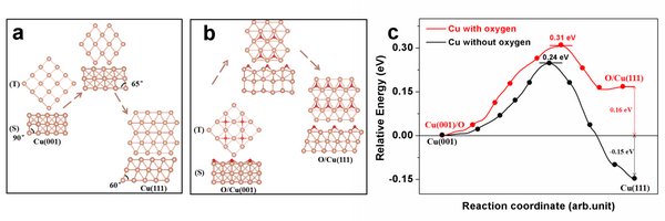
Figure 2: Density functional theory calculations reveal the mechanism of the effect of oxygen on the crystallographic transition of a copper substrate.
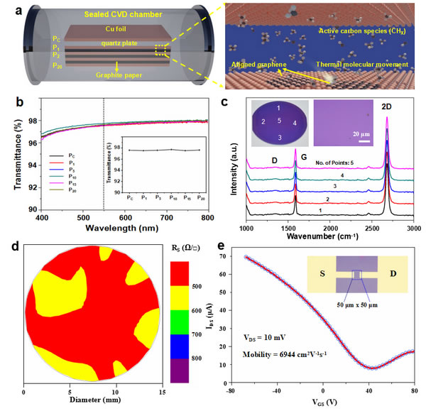
Figure 3: Optical and electrical property characterization of graphene prepared under static atmospheric pressure CVD system. (a) Schematic diagram of mass production of graphene in static atmospheric pressure CVD system; (b) Characterization of light transmittance of graphene film on different copper substrate stacks; (c) Optical and Raman characterization of graphene; (d) The sheet resistance of graphene was characterized; (e) The room-temperature field-effect mobility of graphene was characterized.
Because of its good integration compatibility and low cost advantages in the semiconductor industry, the copper-based surface chemical vapor deposition (CVD) method is considered as the most promising method for mass-producing high-quality graphene. Through nearly 10 years of hard work (2007-2017), copper-based CVD has achieved a series of breakthroughs in large quantities, high quality, and rapid preparation. However, it remains a challenge to be able to simultaneously produce graphenes in rapid, high-volume and high-quality production. There are three main reasons for the analysis: (1) The mismatch between the copper substrate and the graphene lattice leads to an excessively high grain boundary density of the graphene and impairs the physical properties of the graphene; (2) In order to suppress the nucleation of the graphene, the traditional The CVD method is often achieved by reducing the carbon source concentration, resulting in a low growth rate of graphene, between 0.03 μm/s and 0.36 μm/s; (3) Graphene growth as the area of ​​graphene preparation continues to expand The atmosphere becomes non-uniform due to the influence of the flow resistance, resulting in discontinuous or uneven graphene mass production.
In response to the above-mentioned key scientific and technical issues, the Liu Liwei Research Group of the Suzhou Institute of Nanotechnology and Nano-Bionics Research Institute of the Chinese Academy of Sciences in cooperation with Suzhou Gryphon Nanotechnology Co., Ltd., first performed crystal orientation control of the copper substrate, revealing the oxide layer on the copper substrate. Crystalline regulation and mechanism. It was found that the copper surface oxide layer is conducive to the formation of Cu (001) crystal orientation, and after removing the copper surface oxide layer with hydrogen, the copper substrate is rapidly transformed to the Cu (111) crystal orientation (Figure 1), and the density functional is used. Theoretical calculations revealed the mechanism of the effect of oxygen on the crystallographic transition of copper substrates (Figure 2). This work reveals the role of oxygen and hydrogen in the crystallographic orientation of the copper substrate, and it also facilitates the controlled preparation of high-quality graphene with a single crystal substrate. The relevant results have been published in Scientific Reports.7, 45358 (2017).
Based on the above research results, the team proposed to build a high-quality graphene by rapid mass production by constructing a static atmospheric CVD (SAPCVD) system based on molecular thermal motion. The experimental results show that the SAPCVD system can simultaneously prepare batches of optically uniform graphene on 20 copper substrates with a growth rate of 1.5 μm/s. By controlling the lattice mismatch of graphene and copper substrates, the grain boundary density of graphene is effectively suppressed, and the room-temperature field-effect mobility of graphene reaches 6944 cm2 V-1s-1, and the sheet resistance is 500 Ω/□ (Figure 3). ).
Compared to traditional low pressure flowing CVD (LPCVD) or atmospheric pressure CVD (APCVD) systems, the advantages of SAPCVD system for preparing graphene are mainly reflected in three points: First, graphene growth atmosphere is uniform and is not affected by the flow resistance, which is beneficial to Massive preparation of graphene; secondly, the carbon source concentration can achieve uniform monolayer graphene under a large window of 1500%, and it is easier to obtain an optically uniform graphene film; finally, the carbon source can be fully decomposed in the CVD growth chamber, and It can effectively reduce the dependence on vacuum equipment in the process of preparing graphene and reduce the preparation cost of graphene. This work proposes rapid mass production of graphene by static atmospheric pressure CVD technology and Cu(111) single crystal lamination substrate technology, which accelerates the application of graphene in flexible electronic devices. This research result was recently published in Small (DOI: 10.1002/smll.201700651).
This series of work received strong support from the National Natural Science Foundation of China and the Jiangsu Natural Science Foundation.
1. Application:For Solar Frame
2. Dimension: Customized dimension, OEM & ODM
3.Material: A6063, A6061, A3003 and other series alu alloy
4.Suface treatment: Anodizing, polishing, turning ,power coating, mill finish etc
5.Equipment: CNC ,extruding machine, cold drawn machine, heating oven, straightening machine, cutting machine
|
OD |
OD Tolerance |
ID Tolerance |
Roundness |
Straightness |
Circular run-out |
|
φ16-20 |
±0.02 |
±0.02 |
0.01↓ |
0.015↓ |
0.05↓ |
|
φ20-30 |
±0.02 |
±0.02 |
0.01↓ |
0.015↓ |
0.05↓ |
|
φ30-50 |
±0.05 |
±0.05 |
0.02↓ |
0.020↓ |
0.08↓ |
|
φ50-80 |
±0.15 |
±0.10 |
0.05↓ |
0.025↓ |
0.10↓ |
6. STANDARD PACKING:Wooden case/carton
7. Trade Terms
1. Payment: 30% T/T in advance, 70% balance pay before delivery. L/C at sight.
2. Delivery time: 20 days after deposit receiverd. If opening mould, plus 7-10 days.
3. Trade Term can be chosen depending on your requirements.
4. FOB Port: Shanghai
Contact Us
If you want more info.about the aluminum tubes/profiles, please feel free to contact us.
1. Attn: Karina Gu
2. Mobile: +86-18961469527
3. Tel: +86-519-88761254
Aluminum Profile For Solar Frame
Aluminum Profile For Solar Frame,Aluminum Extrusion Solar Frame Profile,Extruded Aluminum Framing,Solar Panel Frames Aluminum
Changzhou YiFei Machinery Co., Ltd. , https://www.yifeialu.com